Sintering technology

Battery-powered vehicles and smart infrastructures
Sintering technology
enable green mobility of today and tomorrow
Sintering technology
Green power delivers the energy for the sustainable mobility revolution
Sintering technology
High-performance semiconductors are the key technology for this.

Benefit from 20 years of experience in electronics, semiconductor and battery production

Your bonding process

For bonding semiconductors, such as IGBTs or SiC MOSFETs with Ag or Au on DBC or AMB substrates or for connecting power modules on heat sinks, metallic silver or copper sintering offers a high-performance solution with maximum reliability. If you are considering sintering as a bonding process, we offer you comprehensive solutions, from consulting, feasibility studies and process implementation to extensive after-sales support.

Consulting

Our process consulting and training services help you to holistically evaluate manufacturing by means of metallic sintering and to derive the process selection and parameters for the production of your end products. Take advantage of our 20 years of experience in the fields of electronics, semiconductor and battery production. We actively support you in the development up to the series production of your products.

Process development​

We have developed a number of pre-processes for sintering that contribute to cost and effort reduction of the overall process. These include hot mounting or tacking of semiconductors, but also dispensing of sintering paste and force-controlled placement of semiconductors or modules on heat sinks. These processes can be adapted to production specifications and product configurations. If this is not sufficient, we develop individual processes, as we have been doing for the semiconductor industry for years.

Sintering

Evaluation

If sintering is your favoured assembly and connection technology, for example in a power module project for e-mobility, we will be happy to support you in the selection of the individual steps, according to your end product, the production volume and the specified cost framework. Based on this evaluation or assessment, we can make suggestions about changes, structure and process optimization and thereby reduce the time-to-market.

Feasibility study​

We carry out feasibility studies for you in our application laboratory. We check the overall solution approach with regard to technical feasibility and application. Depending on whether you want to use metallic sintering for bonding semiconductors to circuit carriers or circuit carriers are to be sintered to base plates, there are different process requirements.

Project management​

Once the evaluations and feasibility studies have delivered a clear picture of the structure of the production process around sintering, we support you in the project management and planning of this assembly and connection process. In doing so, we rely on our broad network and, after agreement with you, bring other partners into the team, e.g. for vacuum brazing or analysis.

Pre-Sintering Processes on Sinter Bonders from Tresky

Prototype and batch size 1 production

In the prototyping phase, in the production of small series or batch size 1, many companies hesitate to invest in their own production line. We will gladly take over this service for you and, with a great deal of technical know-how and our many years of experience, manufacture the prototypes and small batches for you from the first piece on our systems.

Sintering paste application

In order to optimize the entire process of sintering with regard to costs and cycle times, we have developed and implemented our own process technologies. By using a dispenser SQ-Nozzle, large-area deposits of silver or copper sintering paste can be applied sequentially and very precisely. The sintering paste can thus be dispensed onto the substrate in a defined layer height and width in one process step. For process control, the layer thickness of the applied paste depot can be measured directly by laser.

Dispensing of tacking agent

The hot pick and place process is a common method of placing semiconductors for sintering. However, oxides can appear on the bare copper surface of the chip when the substrate is heated. This oxidation can be avoided by conducting the placement at room temperature. In this case, it is necessary to fix the component on the sintering paste to ensure accurate positioning on the transport route to the next process. Therefore, the chips are usually provided with an alcohol-based tacking agent.

Pick & place of components

An important process is the picking and placing of semiconductors. When using sintered matrices, hot tacking is used. This avoids any movement during transport into the sintering press. This process, also called hot pick and place, differs from the standard sintering process with pre-dried and thus no longer sticky sintering paste.

Inline or batch mode production

All DIE bonders from our machine portfolio can be used as sintering bonders. It is possible to work in both inline and batch mode. In inline mode, the DIEs and substrates are automatically transported into the machine and produced in an uninterrupted process. In batch mode, the machine is loaded manually by an operator with DIEs and substrates, e.g. in trays as waffle packs. All the production steps required for the pre-sintering process (tacking) then take place within the machine.

Sintering process Videos

Use of a two track conveyor system​
Play Video

Use of a two-track conveyor system

Unprocessed substrates and SiC MOSFETs can be transported simultaneously into the sintering bonder, by using a two conveyor systems. In this way, the feeding of additional SiC MOSFETs as well as the removal of finished packages can take place automatically and with optimized cycle times.

Dispensing of sintering paste
Play Video

Dispensing the sintering paste using a SQ-Nozzle.

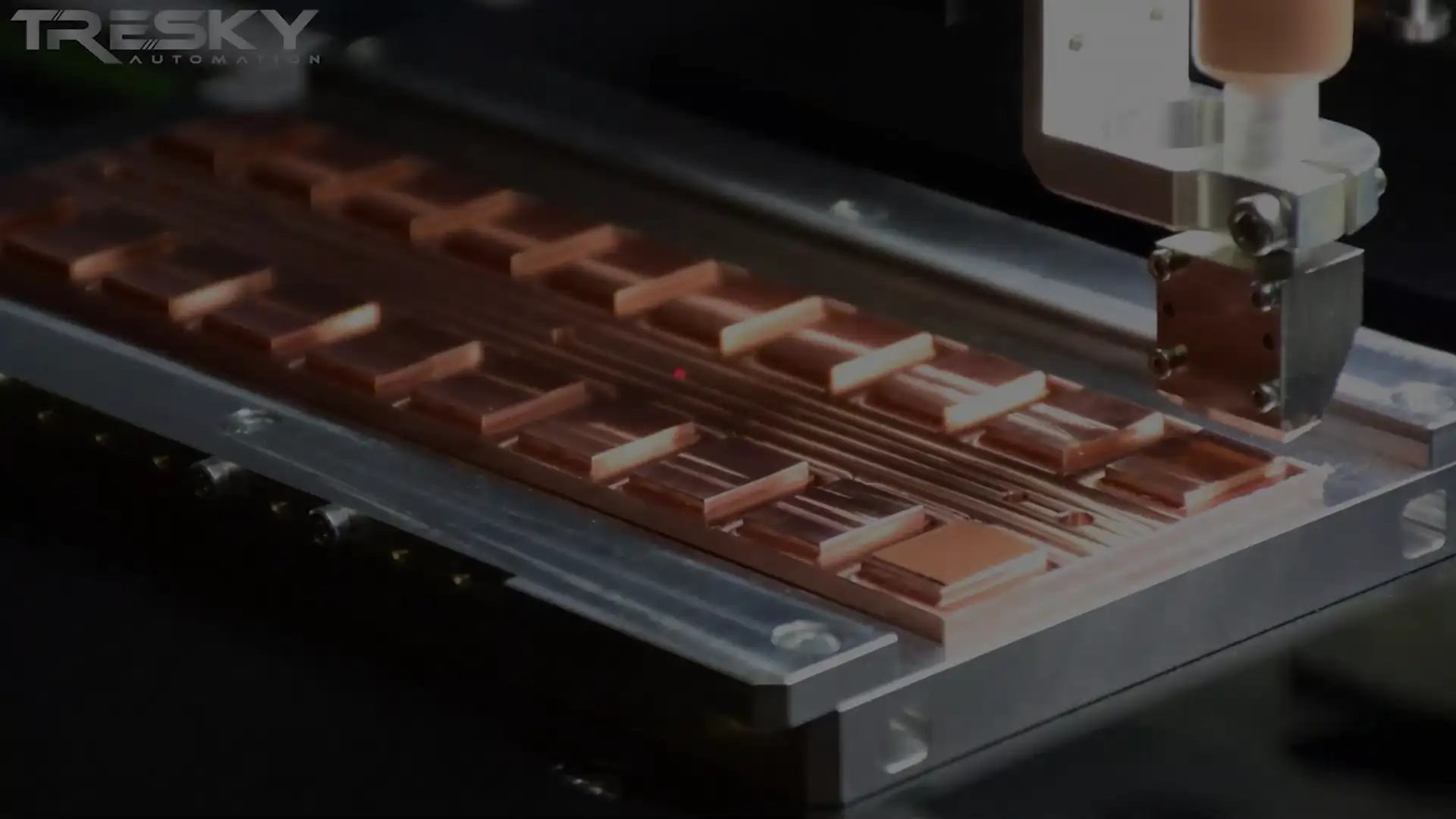
The SQ-Nozzle developed by Tresky allows a sequential and very precise large-area application of deposits of silver or copper sintering paste. The paste is applied to each substrate in one process step, whereby defined layer heights and thicknesses can be applied, which are controlled by measuring the layer thickness.

Layer thickness measurement of sintering paste
Play Video

Layer thickness measurement of sintering paste by laser

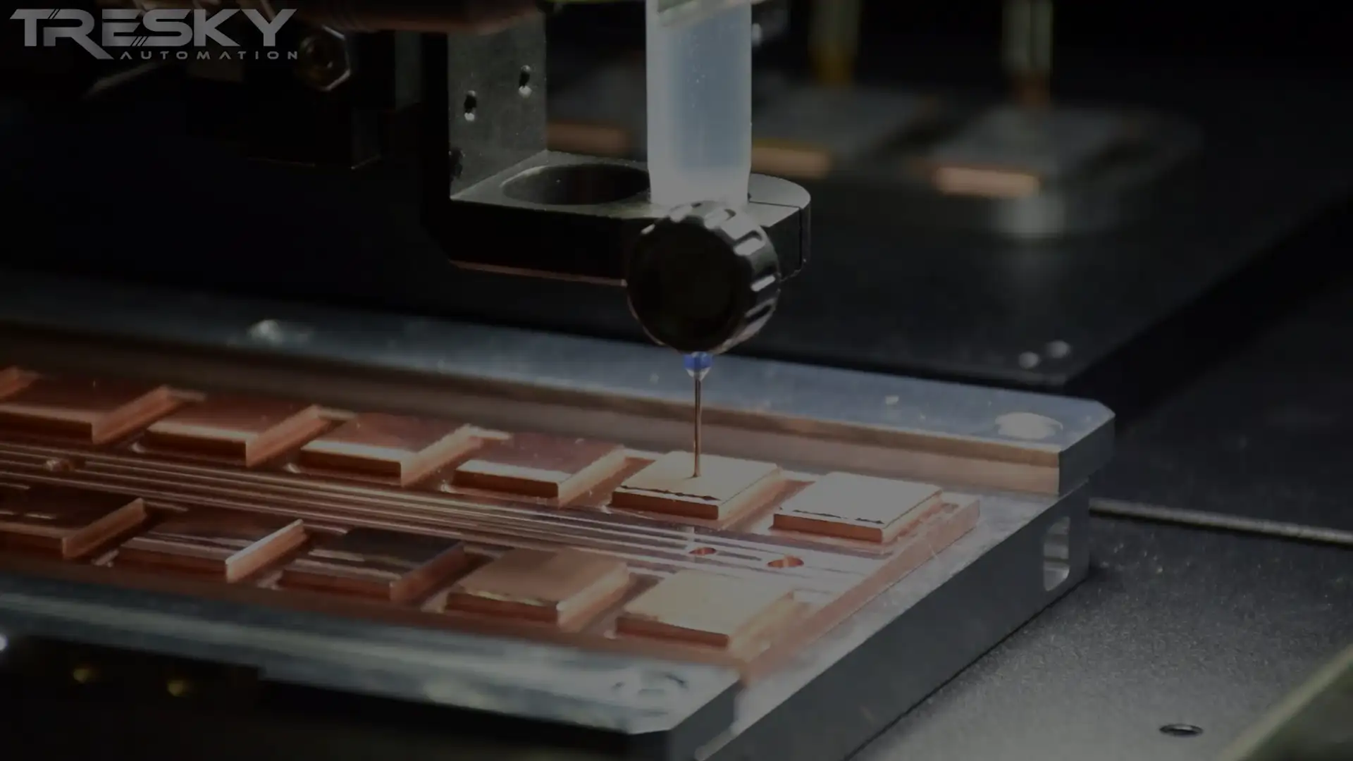
By means of a triangulation laser, the layer thickness of the applied sintering paste is measured without contact. In the process, a distance measurement is carried out by calculating the angle. This guarantees that the dispensing applies the predefined amount of paste and thus reproducible sintering results are achieved.

Pickup and placement
Play Video

Pickup and placement of SiC MOSFETs

After the layer thickness measurement, the SiC MOSFETs are picked from the tray and placed in the applied sintering paste. A previously applied tacking agent fixes the SiC MOSFET in the sintering paste and prevents it from moving during transport to the sintering press.
Application of a tacking agent
Play Video

Applying of a tacking agent to fix SiC MOSFETs

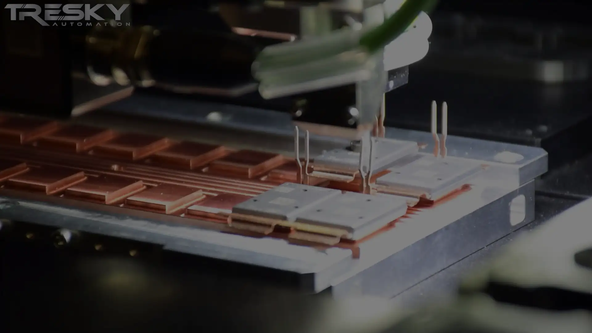
To prevent the SiC MOSFETs from slipping from the sinter bonder during transport to the sinter press, an alcohol-based tacking agent is applied. This evaporates without leaving any residue during the sintering process.

Video